Primero, un juego previo ligero ...
Durante los últimos 4-5 meses, STMicroelectronics ha obligado a los pequeños y medianos fabricantes de microelectrónica a "apretarse el cinturón". No es ningún secreto que durante este tiempo, los chips originales se han disparado de precio, y en los últimos meses, los chips no han estado disponibles en absoluto ... Por lo tanto, debido a la escasez, se acercaron a sus contrapartes chinas.
Por ejemplo, HK32F030C8T6, según el fabricante (Shenzhen Hangshun Chip Technology R&D Co., Ltd.), es una copia completa de su hermano mayor STM32F030C8T6. Así que veamos ...
Abrir la documentación técnica ...
Basado en la descripción: "HK32F030x4 / HK32F030x6 / HK32F030x8. HK32F030 Los chips enumerados son desarrollados por Shenzhen Haohan Tianji Processor Co., Ltd., una subsidiaria de Shenzhen Hangshun Chip Technology Research Co., Ltd.".
Y luego, para ser honesto, ¡estaba encantado! En primer lugar, los chips pueden funcionar en el rango de voltaje de suministro de 2,0 V a 5,5 V. En segundo lugar: ¡la frecuencia máxima de reloj del núcleo es de hasta 72 MHz! Cuento de hadas recto y único !!! Ver por ti mismo !!!:
Pantalla de esos. documento
Oh si. "Hoja de datos" en chino ...
... sigue leyendo !!!
Pantalla de esos. documento
... ...
... RCC_CFGR4, STM' ! "stm32f0xx.h":
typedef struct
{
__IO uint32_t CR; /*!< RCC clock control register, Address offset: 0x00 */
__IO uint32_t CFGR; /*!< RCC clock configuration register, Address offset: 0x04 */
__IO uint32_t CIR; /*!< RCC clock interrupt register, Address offset: 0x08 */
__IO uint32_t APB2RSTR; /*!< RCC APB2 peripheral reset register, Address offset: 0x0C */
__IO uint32_t APB1RSTR; /*!< RCC APB1 peripheral reset register, Address offset: 0x10 */
__IO uint32_t AHBENR; /*!< RCC AHB peripheral clock register, Address offset: 0x14 */
__IO uint32_t APB2ENR; /*!< RCC APB2 peripheral clock enable register, Address offset: 0x18 */
__IO uint32_t APB1ENR; /*!< RCC APB1 peripheral clock enable register, Address offset: 0x1C */
__IO uint32_t BDCR; /*!< RCC Backup domain control register, Address offset: 0x20 */
__IO uint32_t CSR; /*!< RCC clock control & status register, Address offset: 0x24 */
__IO uint32_t AHBRSTR; /*!< RCC AHB peripheral reset register, Address offset: 0x28 */
__IO uint32_t CFGR2; /*!< RCC clock configuration register 2, Address offset: 0x2C */
__IO uint32_t CFGR3; /*!< RCC clock configuration register 3, Address offset: 0x30 */
__IO uint32_t CR2; /*!< RCC clock control register 2, Address offset: 0x34 */
} RCC_TypeDef;
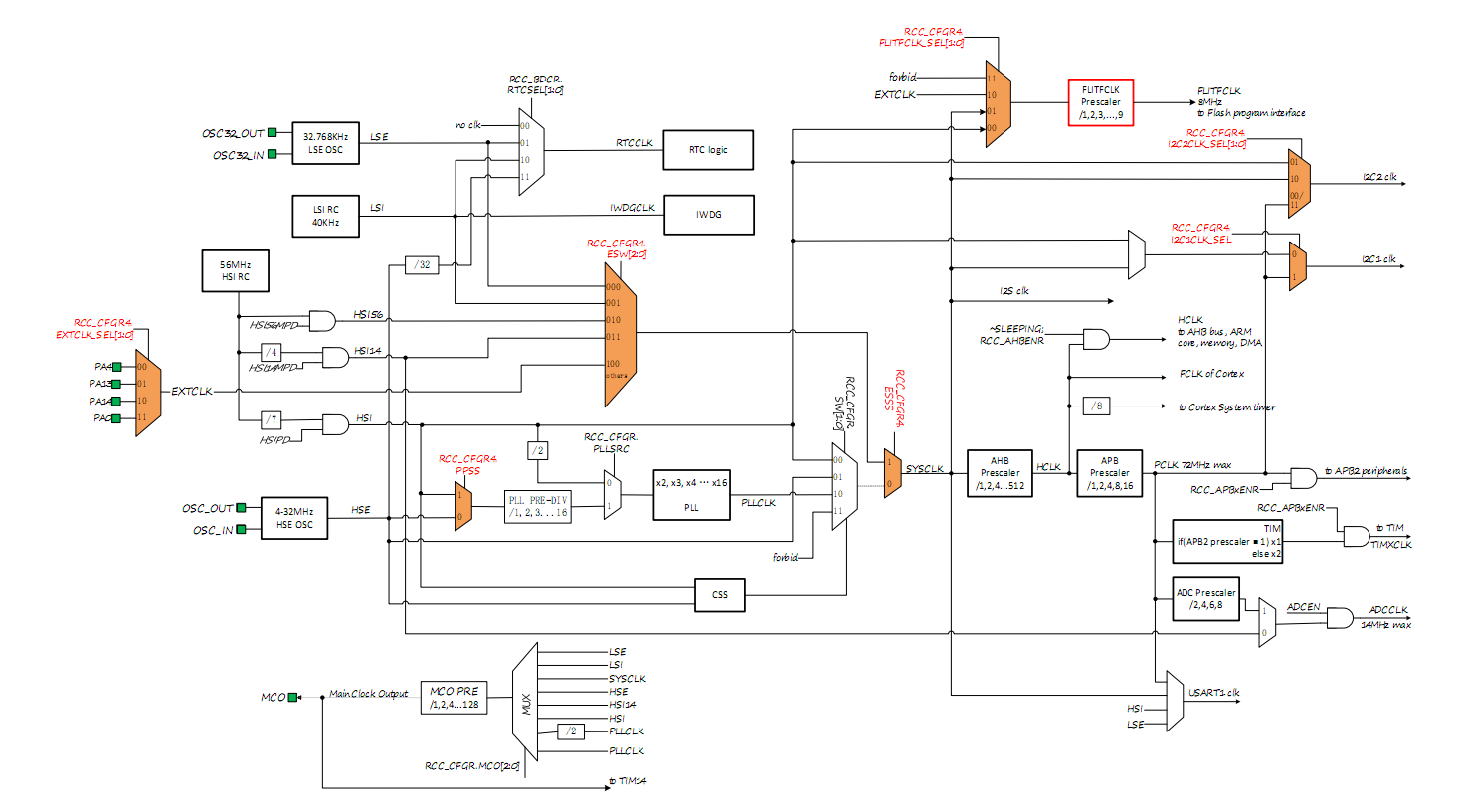
, CFGR4 , :
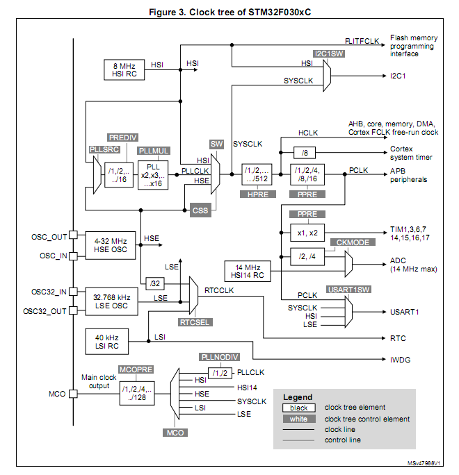
... , STM32F030, CFGR4...
HK32F0_LibraryV1.0.3... :
typedef struct
{
__IO uint32_t CR; /*!< RCC clock control register, Address offset: 0x00 */
__IO uint32_t CFGR; /*!< RCC clock configuration register, Address offset: 0x04 */
__IO uint32_t CIR; /*!< RCC clock interrupt register, Address offset: 0x08 */
__IO uint32_t APB2RSTR; /*!< RCC APB2 peripheral reset register, Address offset: 0x0C */
__IO uint32_t APB1RSTR; /*!< RCC APB1 peripheral reset register, Address offset: 0x10 */
__IO uint32_t AHBENR; /*!< RCC AHB peripheral clock register, Address offset: 0x14 */
__IO uint32_t APB2ENR; /*!< RCC APB2 peripheral clock enable register, Address offset: 0x18 */
__IO uint32_t APB1ENR; /*!< RCC APB1 peripheral clock enable register, Address offset: 0x1C */
__IO uint32_t BDCR; /*!< RCC Backup domain control register, Address offset: 0x20 */
__IO uint32_t CSR; /*!< RCC clock control & status register, Address offset: 0x24 */
__IO uint32_t AHBRSTR; /*!< RCC AHB peripheral reset register, Address offset: 0x28 */
__IO uint32_t CFGR2; /*!< RCC clock configuration register 2, Address offset: 0x2C */
__IO uint32_t CFGR3; /*!< RCC clock configuration register 3, Address offset: 0x30 */
__IO uint32_t CR2; /*!< RCC clock control register 2, Address offset: 0x34 */
uint32_t RESERVED[42]; /*!< Reserved, Address offset: 0x38-dc */
__IO uint32_t HSECTL; /*!< RCC clock HSE control, Address offset: 0xe0 */
uint32_t RESERVED1; /*!< Reserved, Address offset: 0xe4 */
__IO uint32_t CFGR4; /*!< RCC clock control register 4, Address offset: 0xe8 */
__IO uint32_t AHBENR2; /*!< RCC clock configuration ahb, Address offset: 0xec */
} RCC_TypeDef;
... (uint32_t RESERVED[42]; /*!< Reserved) ?
, ! !!! (... USB STM32F0xx...) , :
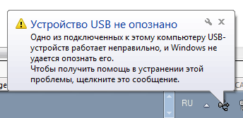
, STM32F030, :
, STM HK USB ... ... USB ARM, : "NOP
performs no operation and is not guaranteed to be time consuming. The processor might remove it from the pipeline before it reaches the execution stage. " NOP "" ... , ?
ARM!!!
HK "" . .
...
System Tick Timer! , , Watchdog ( - ). , . - :
(STM32F030):
asm_usb_tx
PUSH {R4-R7,LR} ;10
LDR R3,DataTable+0x08 ;6
LDR R2,DataTable+0x14 ;6
STR R2,[R3, #+0x18] ;5
LDR R4,[R3, #+0] ;5
MOVS R5,#+5 ;4
LSLS R5,R5,#+22 ;4
ORRS R5,R5,R4 ;4
STR R5,[R3, #+0] ;5
MOVS R7,#+0 ;4
ADDS R1,R1,#+1 ;4
ut_0
LDRB R5,[R0,#+0] ;5
NOP ;4
NOP ;4
SUBS R1,R1,#+1 ;4
BEQ ut_2 ;4
MOVS R6,#+8 ;4
LDRB R4,[R0,#+0] ;5
ADDS R0,R0,#+1 ;4
"" (HK32F030):
asm_usb_tx
PUSH {R4-R7,LR} ;10
LDR R3,DataTable+0x08 ;6
LDR R2,DataTable+0x14 ;6
STR R2,[R3, #+0x18] ;9 GPIOA->BSRR
LDR R4,[R3, #+0] ;8 GPIOA->MODER
MOVS R5,#+5 ;4
LSLS R5,R5,#+22 ;4
ORRS R5,R5,R4 ;4
STR R5,[R3, #+0] ;6 GPIOA->MODER
MOVS R7,#+0 ;4
ADDS R1,R1,#+1 ;4
ut_0
LDRB R5,[R0,#+0] ;9
NOP ;4
NOP ;4
SUBS R1,R1,#+1 ;4
BEQ ut_2 ;4->8
MOVS R6,#+8 ;4
LDRB R4,[R0,#+0] ;9 Load transmited Byte
ADDS R0,R0,#+1 ;6 Increment TX Buffer Pointer
... LDR/STR Immediate Value... , - - , , - ... , 72 MHz, .
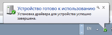
6 9. , , , , "" " ". .
:
...HK STM...
, , STM, , , GPIO. , .
HK , STM, ADC/TIM/USART/IWDG/GPIO, - , , .
72MHz "" / . "" "" . , STM' 48MHz, HK 72, " " 48MHz STM HK 72MHz, 72 != 48, , , .
.
! , .